Recent discoveries from the University of Chicago have ignited a new wave of excitement in the field of material science, particularly regarding antiferroelectric materials. These materials have unique electrical properties that hold immense promise for future technologies spanning energy storage, advanced sensors, and highly efficient memory devices. The true potential of these materials can only be realized through an intricate understanding of their electronic properties, making the new imaging techniques developed by researchers not just a breakthrough but a necessity for technological advancement.
Antiferroelectric materials are fascinating for their arrangement of electric dipoles, which allow their charges to negate each other, leading to no net polarization. This intricate balance yields a complex interplay of physical characteristics that researchers aim to harness. With various configurations of dipoles resulting in unique “domains,” the challenge has always been how to observe and manipulate these domains effectively to unlock the materials’ full potential.
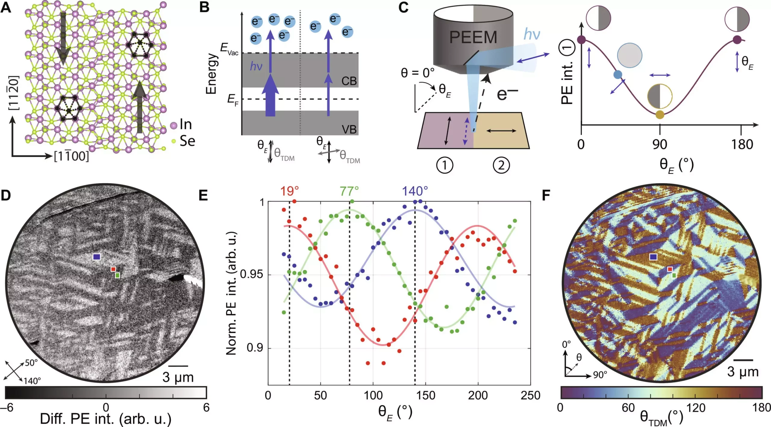
The Imaging Breakthrough: A New Dawn for Antiferroelectric Materials
Sarah King, an Assistant Professor of Chemistry and senior author of the study, emphasized the transformative nature of their discovery: “We demonstrated a new method for emerging antiferroelectric materials on the nanoscale.” Such a statement encapsulates the transformative power of their findings; the ability to image these materials with unprecedented resolution allows for an in-depth exploration of their electronic attributes. Traditionally, the lack of resolution in standard imaging techniques led to considerable hurdles in understanding and characterizing antiferroelectric materials, but King’s lab has pushed through these barriers by introducing innovative methodologies.
At the heart of this advancement is an advanced microscopy technique known as polarization-dependent photoemission electron microscopy. By utilizing polarized laser light in combination with electron imaging, the research team successfully revealed the intricate arrangements of electric dipole domains within materials such as indium selenide, a widely studied antiferroelectric substance. This convergence of techniques promises not only to illuminate the domestic nature of antiferroelectric materials but also to reshape our understanding of material interactions at the nanoscale.
Why This Matters: The Implications of Enhanced Imaging
The implications of this research are profound. The ability to visualize and manipulate domains in antiferroelectric materials facilitates a deeper inquiry into their properties, notably their response to applied electric fields. The process of switching these materials to higher energy states—where the electric dipoles interact differently—offers a glimpse into their potential applications; this could fundamentally change the landscape of electronics and energy storage technologies.
Not only can these insights allow scientists to better engineer materials for existing technologies, but they also pave the way for entirely new applications—whether in renewable energy solutions or ultrafast electronic devices. As King rightly pointed out, understanding the interactions between various material properties can highlight the significance of order and domain formation. This kind of knowledge could foster advancements we have yet to conceive, opening new research avenues and applications.
The Collaborative Spirit Driving Innovation
Another striking aspect of this research is the collaborative effort brought together by students and postdoctoral researchers, fostering a culture of innovation that is crucial for scientific advancement. The success of this particular study showcases the importance of diverse perspectives in navigating complex scientific questions. Graduate students like Joseph Spellberg, and others alongside their experienced peers, exemplify the synergy necessary for breakthroughs in material science.
As research institutions continue to champion such collaborative environments, the acceleration in uncovering novel materials—like antiferroelectric compounds—will certainly benefit. By catalyzing new partnerships, organizations can enhance knowledge sharing, streamline research processes, and ultimately cultivate groundbreaking innovations that challenge the boundaries of current material usage and functionality.
In the rapidly evolving landscape of technology, these cutting-edge imaging techniques provide more than just clarity—they offer a new lens through which to explore the future. Exciting possibilities lie ahead, driven by profound discoveries that not only promise to refine existing technologies but fundamentally redefine our interaction with material science. As scientists like Sarah King lead the charge, the excitement surrounding these advances is palpable, suggesting a future rich in potential and innovation.
Leave a Reply